
Transistors are amplifiers in which a small signal controls a larger signal. One type of transistor is a junction field-effect transistor (JFET). JFET transistors provide a good picture of how transistor circuits work, so it’s a good idea to start with them when studying circuit analysis.
The two primary types of transistors are bipolar transistors and field-effect transistors. The field-effect transistor is a little simpler than the bipolar kind. You can classify field-effect transistors, or FETs, in two ways: junction field-effect transistors (JFETs) and metal-oxide-semiconductor field-effect transistors (MOSFETs).
Typical transistors have three leads. In the case of a JFET, a voltage on one lead (called the gate) is used to control a current between the two other leads (called the source and the drain). The gate voltage needs to be referenced to some other voltage, and by convention, it’s referenced to the source terminal.
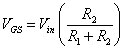
Here is the JFET symbol and its corresponding dependence model. The gate, drain, and source labels (G, D, and S, respectively) are normally omitted, but are included here for reference.
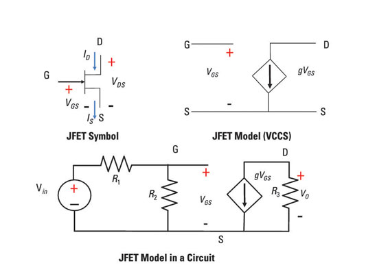
In the sample circuit, VGS refers to the voltage between the gate and the source, ID is the current into the drain, and IS is the current out of the source. No current flows into the gate when it’s operating under normal conditions, implying that the drain current ID is equal to the source current IS.
A useful JFET model, which you see on the upper right of sample circuit, uses a voltage-controlled current source (VCCS). The model is part of the circuit shown at the bottom of the figure.
For the circuit shown here, you need to find the ratio between the output voltage VO and the input voltage Vin. The dependent source is a voltage-controlled current source, so its current is gVGS. So at the output terminals of the dependent source model, the output voltage VO is a result of the following equation using Ohm’s law (v = iR):
Vo = (-gVGS)R3
The minus sign appears because the current through resistor R3 flows in the opposite direction of the voltage polarities of the output voltage VO. You can find the voltage VGS on the input terminals of the dependent VCCS model.
Because the devices are connected in series on the input side of the circuit, you can use the voltage divider technique, as follows:
Now substitute this expression for VGS into the Ohm’s law equation for output voltage VO. You get the following input-output relationship:
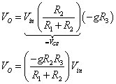
To see the amount of amplification using this circuit, try plugging in some numbers. Suppose g = 1.8 milliamps per volt, R1 = R2 = 1 kΩ, R3 = 10 kΩ, and Vin = 1 volt. The amplifier output is
The input is amplified by –9 at the output of the dependent source. Awesome! The signal is bigger because an external voltage source made this JFET transistor work as an amplifier. The minus sign means that the signal is inverted or upside down, which is no problem because it doesn’t change the sound quality of your music.